How Ceramic PCBs Are Manufactured
Ceramic PCBs Are Manufactured
Ceramic PCBs are emerging as an effective solution for modern electronic products and the assembly technology of surface mount components (SMDs). These circuit boards can withstand high temperatures, offer better electrical properties and provide excellent thermal management. They also feature superior signal integrity and EMI/EMC performance, making them ideal for harsh environments.
In addition to their superior thermal, mechanical and chemical resistance properties, ceramics have exceptional conductivity, enabling them to effectively dissipate heat generated by electronic components. This unique feature makes them suitable for use in demanding applications like automotive, aerospace and power electronics.
Conventional organic laminates used in conventional ceramic pcb board are challenged by high temperature environments because of their low thermal conductivity. On the other hand, high-temperature co-fired ceramic (HTCC) pcb boards can withstand higher temperatures without losing their structural integrity and electrical performance. They are manufactured by mixing raw materials such as ceramic powders, solvents, plasticizers and lubricants with aluminum oxide and then baking them at elevated temperatures.
How Ceramic PCBs Are Manufactured
HTCC boards are available in various formats, with different thicknesses and copper-to-aluminum ratios. Depending on the specifications of the application, the board can be designed with a variety of features and layouts. This type of specialized PCB is often used in power electronics, automotive and aerospace applications.
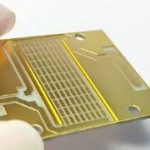
Thick film copper circuit technology is the most popular and widely used fabrication method for ceramic pcb boards. This technique involves printing alternate layers of gold and dielectric pastes on the substrate, followed by a process called baking. This step prevents the copper from oxidizing and allows manufacturers to integrate interchangeable conductors, resistors, semiconductors and capacitors on the board.
Other fabrication techniques for ceramic pcbs include screen printing, inkjet printing and laser etching. After completing these steps, manufacturers apply a layer of conductive material, usually metal pastes that contain silver or gold particles, to the surface of the substrate. Vias, which are small holes that connect different layers of the circuit board, are then drilled using a laser or mechanical drill. The completed substrate is then fired in a high-temperature furnace to sinter the conductive layer and fuse it to the rest of the ceramic.
Depending on the application, the finished ceramic circuit board may need to be tested and verified to ensure that it meets its design specifications. This testing includes continuity checks, electrical tests and possibly environmental inspection. In some cases, the pcbs may also need to be coated with polymer materials or encapsulated to protect them from chemicals and environmental conditions. Finally, the finished circuit boards are subjected to a series of visual and functional tests before being shipped to customers.